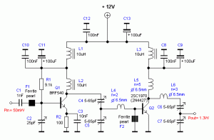
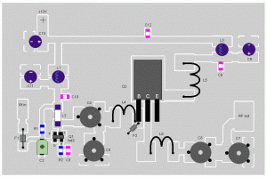
This diagram is a schematic diagram of RF amplifier circuit. The circuit will amplify the RF signal about 10 times, 100mW input power to 1.3W output power. It use a general NPN RF transistor 2SC1970. You may apply other transistors, for example 2N442.
Circuit Works:
RF system and specially in RF amplifiers, this circuit really essential to have a stable power supply and getting sure you will not get any RF out on the power line. The Capacitor C12 and C13 will stabilise the DC power supply. L1, C10, C11 and L3 with C8, C9 will also avoid RF from leaking out to the powerline and trigger oscillation or disturbances. L1 and L3 need to be ferrite chokes or inductance’s about 1 to 10 uH.
Transistor Q1 will act as a buffer amplifier, simply because we do not wish to load the earlier stage to much.
The input RF signal is passin C1 and F1 which is a small ferrite pearl where the wire just passing through.
F1 with C2 will act as an impedance matching for Q1.
F1 could be substituted with a coil as L4, but during test, there is identified that the ferrite pearls gave most effective performances.
L2 is not a vital component and any coil from 2-10uH is adequate. Q1 will amplify the input signal from 50mW to about 200mW.
Q1 can amplify even more, however it does not have to do that since 200mW is fine for the final transistor.
If you need more power, you are able to reduce the value of resistor R2.
When you take a look at Q2, you’ll also see a ferrite pearl F2 at the base to emitter. This ferrite pearls is work to set the DC voltage to zero and be a high impedance for RF signals. I wounded the wire 4 times around this small ferrite pearl. You’ll be able to replace it with a 1uH coil or more.
C4, C5 and L4 forms an input matching unit for the transistor. Not much we can do about that?
At the output of the final transistor Q2 you’ll find two coils L5 and L6. Together with C6 and C7, they form an impedance unit for the antenna and also for the transistor.
Circuit Notes:
- You may apply other power transistor as 2SC1971 (6W) to obtain higher output power.
- 1.3W will still get your RF signal fairly far and you adviced to make use of a solid 50 ohm resistor as dummy load. Ensure it can take up to 5-10W to prevent overheating on the resistor dummy load.
- You have to use an antenna or 50 ohm dummy resistor during the testing, no output loads means transistor to be burned.
1.3W RF Amplifier circuit source: http://hem.passagen.se/communication/1wpa.html


