
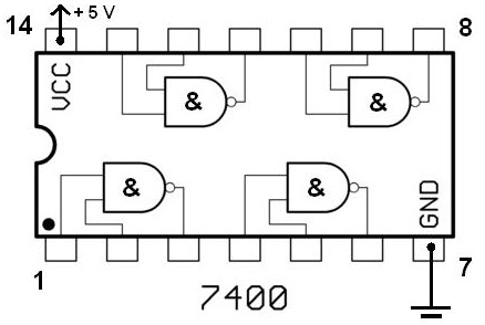
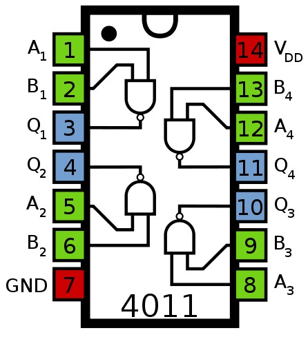
The following scheme is the clock generator circuit diagram which build based on NAND Gate logic IC. You may use IC 7400 or 4011 for this circuit. The 7400 is a Transistor-Transistor Logic (TTL) type, while 4011 is Complementary metal?oxide?semiconductor (CMOS) type. IC 4011 is cheaper than 7400 but the 7400 is faster than 4011.

Circuit Notes:
- Excellent clock generator to drive 4017 type CMOS circuits.
- R1 = 10K to 10M, C1 = 100pF to 47uF.
- Fo is ? 1KHz when R1 = 100K and C1 = 10nF.
- You must use regulated 5V input voltage for 7400, while CMOS 4011 can be from 5 to 15V. Regulated power supply with LM7805 will be great to supply this circuit (with 7400).
Below images are the pin assignment for NAND Gate TTL IC 7400 and NAND Gate CMOS IC 4011:


")