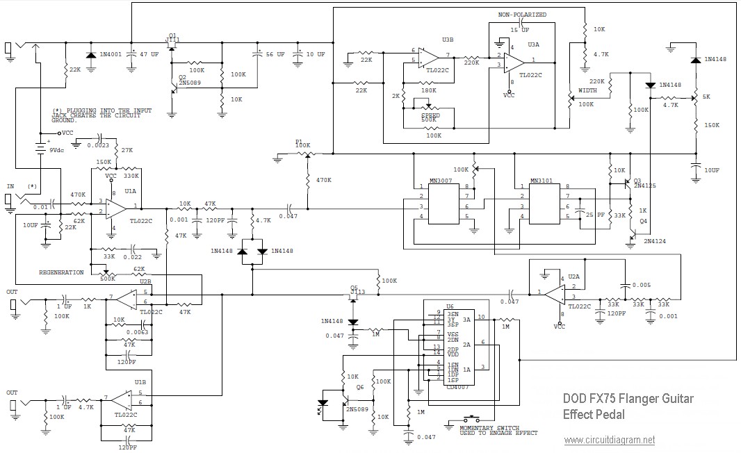
DOD FX75 Flanger Guitar Effect Pedal circuit diagram
Technical info:
– Specifications (1984): Input impedance = 500 k Ohms, Output impedance = 1 k Ohms; Gain = 0 dB; Delay Time = 0.5-6 ms; Signal-to-noise ratio = 90 dB
– Specifications (1986): same as above, plus Maximum Input Level = 4 V P-P, Bandwidth = 40 Hz-16 kHz (dry), 90 Hz-12 kHz (delay); Sweep Speed = 0.1-8 Hz
– Official schematic provided with pedal by DOD (dated 10/14/1984)
– Notable IC chips: MN3007 BBD chip driven by a MN3101 clock generator/driver CMOS chip; three TL022CP op amps (early versions) or one TL022CP and two 1458-type op amps (later versions)
– Internal trim pots: three; however, we do not recommend messing with trim pots

