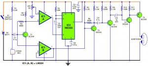
This is the circuit diagram of electronic hearing aid featured with sensitive sound detection and energy saving, so this hearing aid will work in the long term with a 9V batery battery cycle. The common hearing aid circuits consume the battery energy continuously once they are turned on. This smart electronic hearing aid saves battery power by switching on the sound amplifier section only when sound is detected. The sensitivity of the detection section and the ‘on’ time duration of the sound amplifier circuit can be set by the user. The circuit also uses only a single condenser microphone for to detect the sound and amplify the sound signal.
This electronic hearing aid circuit consists of a condenser microphone, earphone, and sound detection and amplification sections. The block of sound detection section used a quad op-amp IC LM324 (IC1(A)) and a timer NE555 (IC2). The sound signal received at the condenser mic is pre-amplified by transistor BC549 (T1). The voltage at its collector is fed to the inverting terminal (pin 2) of op-amp IC1(A), which is utilized as a comparator. The reference voltage (Vref) at the non-inverting terminal (pin 3) of IC1(A) is set with preset VR1. The preset is also used to control the sensitivity of the sound signals received by the circuit. The output from pin 1 of IC1(A) is fed to the trigger input (pin 2) of timer NE555, which is configured in monostable mode.
When sufficient sound signal strength is detected at the base of transistor T1, the pulsating voltage at its collector exceeds the reference voltage at pin 3. As a result, output pin 1 of IC1(A) goes low. The low output from IC1(A) triggers the NE555 timer and its output goes high for a preset duration. R4 and C2 are the timing components for setting the time duration. The high output of the timer is directly used as the power source for the sound amplifier section.
The block of sound amplifier section is built around transistors T2 through T5. The last amplifier stage T5 (PNP transistor BC558) drives the earphone. The sound signal received from the mic is fed to the non-inverting pin of the second op-amp of IC1(B) which is wired in unity follower configuration. The unity follower mode resolves the problem of impedance mismatch which would have occured if the output of the mic is fed directly to amplifier stage. The output from pin 7 of IC1(B) is fed to the base of transistor T2. The weak signal received at transistor stage T2 is further amplified by transistors T3, T4 and T5. An earphone to listen to the sound is connected between the collector of T5 and ground. It is recommended to use a mono earphone with volume control attached.
With 9V battery, when sound is detected through the condenser microphone, the amplifier section is automatically triggered and the current consumption of the circuit is about 96 mA. When the amplifier circuit is ‘off,’ the circuit draws a current of about 6 mA only, thus will be save the battery power usage.


Can anyone tell me if this can be used like Electronic Ear Protection?? ore modified to do so?
ore can anybody tell me where to find a diagram for this?