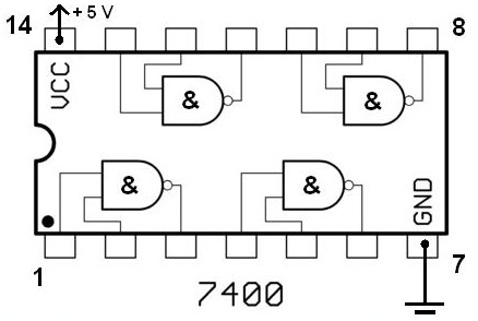
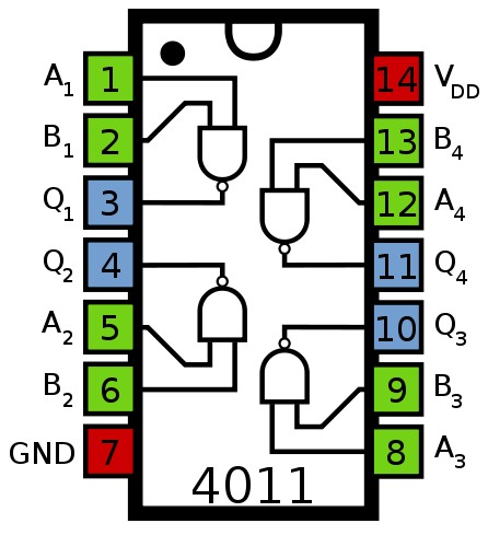
The following scheme is the clock generator circuit diagram which build based on NAND Gate logic IC. You may use IC 7400 or 4011 for this circuit. The 7400 is a Transistor-Transistor Logic (TTL) type, while 4011 is Complementary metal?oxide?semiconductor (CMOS) type. IC 4011 is cheaper than 7400 but the 7400 is faster than 4011.
Circuit Notes:
Below images are the pin assignment for NAND Gate TTL IC 7400 and NAND Gate CMOS IC 4011:
Do you have a bicycle..? why don't try to build this circuit..?. Powered using battery…
This is the circuit diagram of 3A switching power supply regulator: Simple and cheap, the…
Here is the remote control tester circuit. This circuit is really a simple and easy…
This is the circuit diagram of current output multiplier designed for regulator IC LM78xx. By…
The following diagram is the FM tracking transmitter based on 4 transistors. No additional notes…
This is the circuit diagram of white line follower toy. The actuator of the toy…